Back
Expo Plus Pass
Thought Leadership Pass
All-In Pass
Session: Ecosystem Readiness for Scaling and Lithography at 3nm and Below
Holistic Patterning to Enable Manufacturing for 3nm and Beyond
Thursday, July 14, 2022
10:55am – 11:15am
Location: TechTALKS Stage, South Hall, Lower Lobby

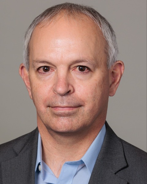
Michael Lercel, PhD
Senior Director Strategic Marketing
ASML, Connecticut, United States
Speaker(s)
Semiconductors have enabled ever-increasing efficiency in compute and storage of information, as a result of decades of cost-effective scaling of device density and generations of new device technologies. We believe that continued advances in holistic patterning will enable cost-effective scaling of semiconductor devices to continue with the 3nm node and beyond.
We present here key developments across the holistic product portfolio: the extreme ultraviolet (EUV) lithography roadmap with its 0.33 numerical-aperture (NA) platform and the next-generation 0.55 NA (High-NA) platform, the deep ultraviolet (DUV) roadmap including cutting-edge immersion lithography and cost-efficient mature systems, and key innovations across optical metrology, electron-beam metrology and inspection portfolio , and in computational lithographic technology.
In high-volume manufacturing, the ultimate lithographic performance is only realized by the holistic combination of exposure systems , metrology and inspection tools, and computational-lithographic algorithms. This includes process window optimization during setup, accurate measurement of process capability, and active control to stay within the patterning process window.
